Structuring and Polishing with USP Laser Radiation

Flexible and Hard – DLC-Coating of LASER-Structured Elastomers
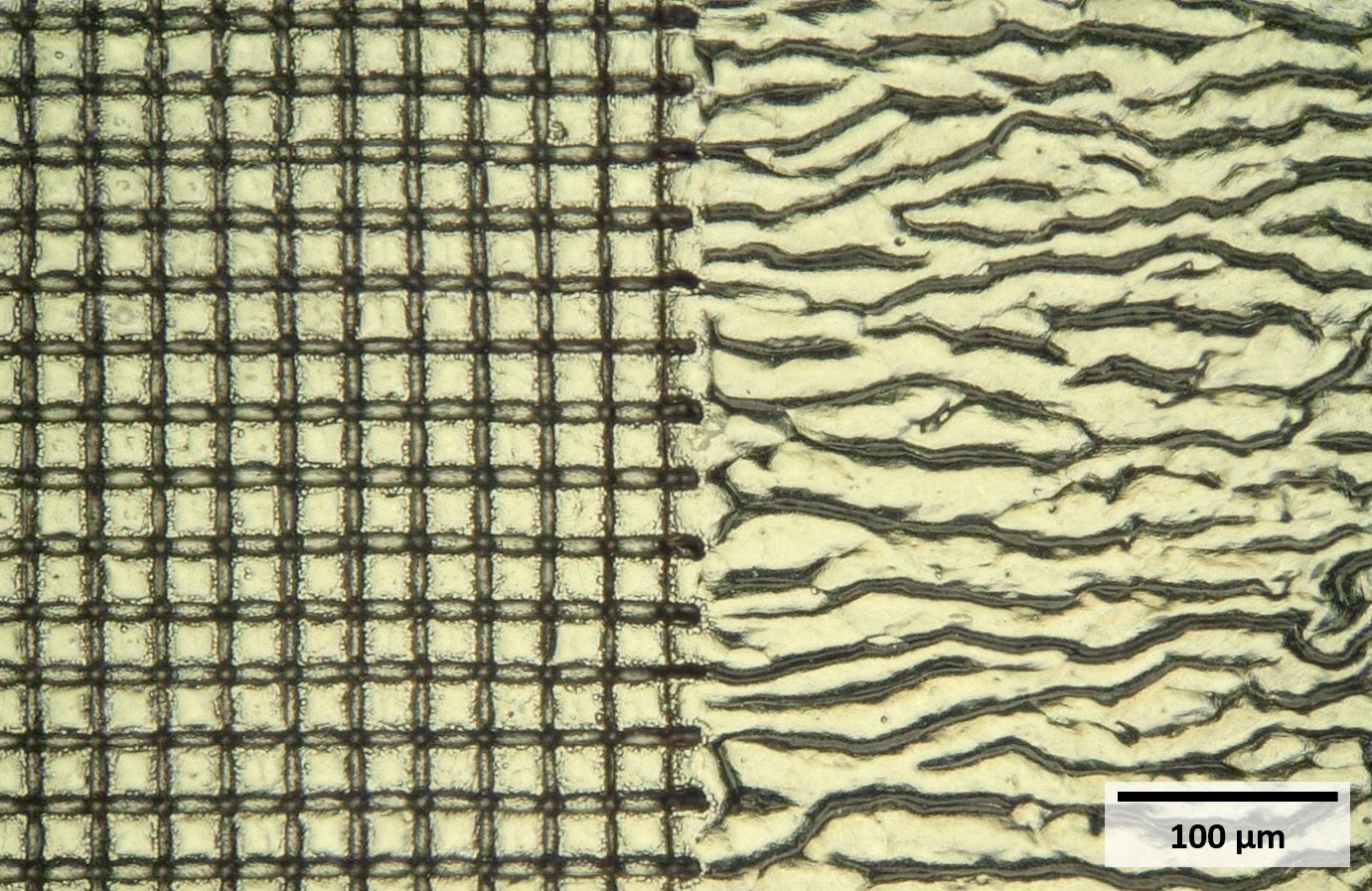
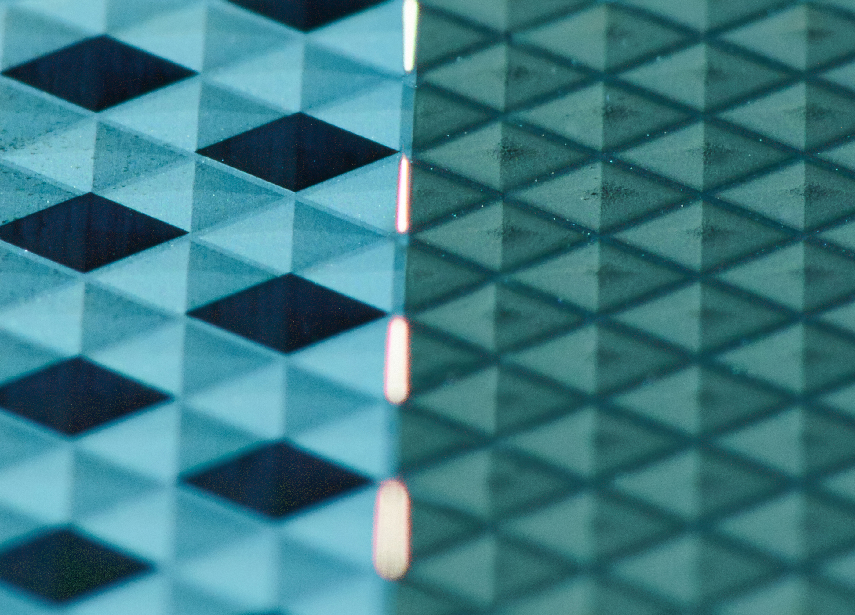
Comparison of coated and structured (left) and unstructured (right) elastomer substrate.
© Fraunhofer ILT, Aachen, Germany.
Comparison of coated and structured (left) and unstructured (right) elastomer substrate.

DLC-coatings show great potential in terms of friction reduction and life-time extension of highly stressed polymer components, such as bearings or elastomer seals. However, a distinct crack morphology is intrinsic to a DLC-coating on elastomer substrates. Due to the different ductility of polymer substrate and DLC coating, the coating is further fragmented under load up to delamination.

Fraunhofer ILT and Fraunhofer IWM achieved a predefined morphology of the DLC-coating by selectively laser-structuring of elastomer substrates. Further fragmentation can thus be avoided, achieving a higher resistance to delamination. The combination of laser structuring and DLC coating enables the production of low-friction and at the same time flexible, highly stressed elastomer components.

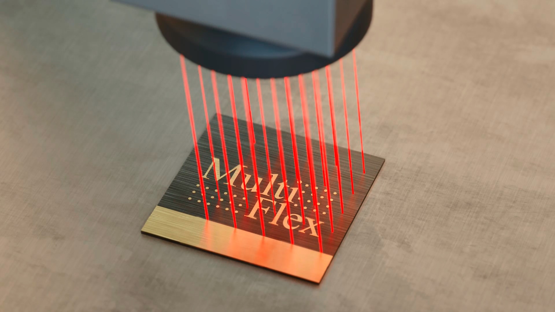
Concept video: Multibeam processing with 1kW and 64 partial beams in the MultiFlex project

Parallel processing of a surface with several laser beams.
© Fraunhofer ILT, Aachen, Germany.
Parallel processing of a surface with several laser beams.

The application of ultrafast laser processes on large surfaces is often not feasible today due to a high process duration and the associated costs. The aim of the MultiFlex project is to tackle this challenge by significantly increasing the productivity of ultrafast laser processes through flexible multi-beam processing.

After the conceptual phase of the project was completed in spring 2020, we are now able to give an insight into our project and the machine concept for the MultiFlex approach to laser processing in a video. Join us on a journey that starts with the idea behind MultiFlex, follows the laser beam through the machine and highlights some of the many possible applications!

Photonic Process Chain for efficient ultrashort pulse surface texturing

Photonic process chain with USP structuring, cleaning and polishing.

Industrial laser texturing is currently still dominated by nanosecond lasers. New approaches show that by means of ultrafast laser sources the productivity of nanosecond lasers is exceeded by a factor of 4 while maintaining the same quality. A removal rate of up to 20 mm³/min with a surface roughness of Ra = 1.5 µm can be achieved. Even roughnesses of < 0.5 µm can be achieved with a ablation rate of up to 10 mm³/min. The photonic process chain shows that with the universal tool of an ultrafast laser, subsequent processes such as cleaning and polishing can also be carried out in the same machinery without time-consuming set-up or re-clamping of the workpiece.

Laser structuring at triple the productivity

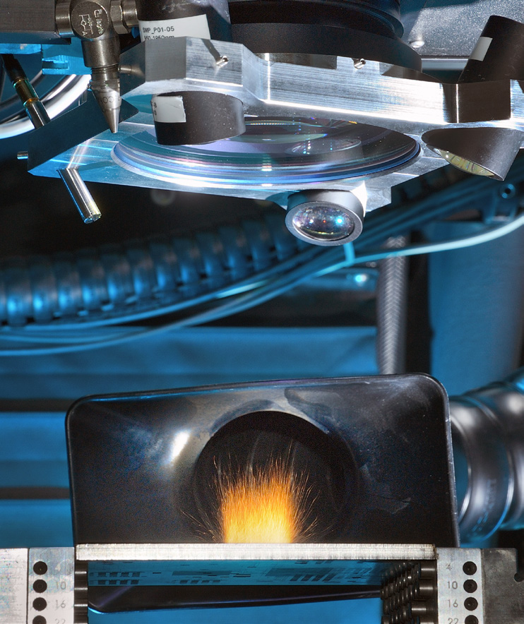
Process of USP laser cleaning and USP polishing after structure generation.
© Fraunhofer ILT, Aachen, Germany / Voker Lannert.
Process of USP laser cleaning and USP polishing after structure generation.

Car makers currently use a variety of methods to emboss plastic panels for vehicle interiors. However, manufacturing the tools required for this purpose is an extremely time-consuming process. This situation can be improved using a new laser machine that triples the rate at which these tools are produced while facilitating even more complex structures. The expertise required for the various components and processes was developed as part of the “eVerest“ project in collaboration with partners from research and industry.

The machine’s new process control system enables the execution of different processing steps in the same clamping. For examplea photonic process chain can be created by arranging the laser structuring, laser cleaning and laser polishing processes in sequence.

Color coding through micro and nanostructures

Color effects generated by interference structuring.
© Fraunhofer ILT, Aachen, Germany.
Color effects generated by interference structuring.

The visible color spectrum between 400 nm and 800 nm is a section of the electromagnetic spectrum whose individual spectral components are perceived as color by the human eye. If the spectrum of a light source strikes the periodic pattern of a micro- or nanostructured surface, its spectral components are diffracted under different angles. Therefore, the surface appears in a different color depending on the angle of view. With ultrashort pulsed laser radiation, defined structures can be generated on surfaces that reflect or absorb specific parts of the color spectrum. This project aims to generate a predefined colored pattern through an automated microstructuring process on different materials.

In addition to decorative applications, the structures can be used for the production of technical surfaces in the medical, biotechnological field or security marking in production.

Microstructuring as part of the networked adaptive process chain

Multi-sensor system for process monitoring.
© Fraunhofer ILT, Aachen, Germany.
Multi-sensor system for process monitoring.

As part of the International Center for Networked, Adaptive Production ICNAP, laser-based microstructuring is being integrated as a final step in a process chain for tools for automotive applications produced in lot sizes of one. Here, a distinction is made between two processes: faster ns- and more precise ps-structuring. During the production process, it is decided which process combination provides the best results – on the basis of important criteria such as machining time, costs and accuracy, surface roughness and the current machine condition. Fraunhofer ILT is developing a multi-sensor system that collects and analyzes the necessary data in order to enable users to detect defects and make decisions based on them in real time.

Application fields for the real-time process monitoring system

  • microstructuring in automotive, lighting and aerospace industry
  • manufacturing processes can be integrated into I4.0 process chains
  • scanner-based laser applications


Large surface microstructuring with UV laser radiation

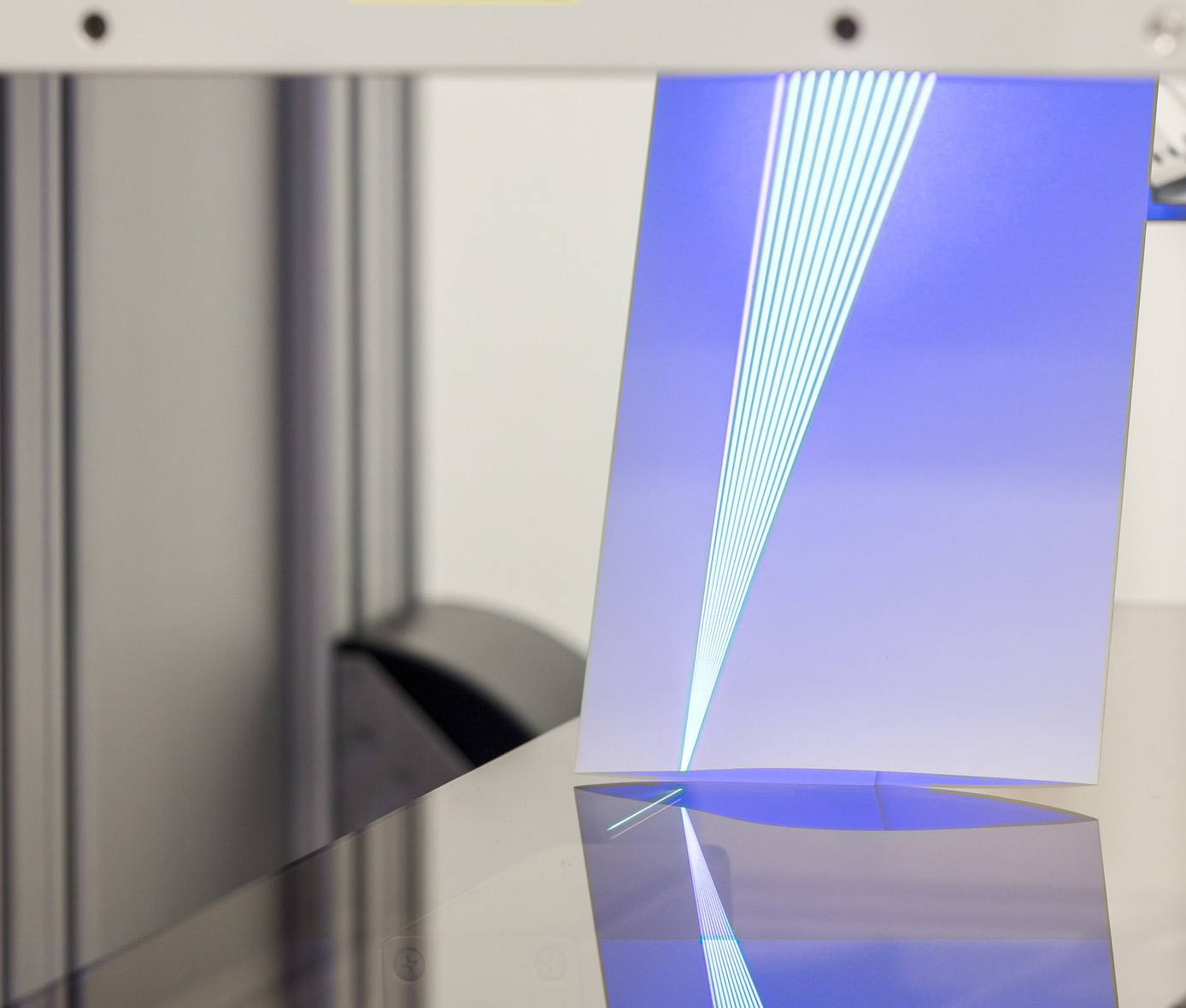
Line beam with 155 x 0.3 mm field size.
© Fraunhofer ILT, Aachen, Germany.
Line beam with 155 x 0.3 mm field size.

Using UV laser radiation to selectively ablate and modify micro- and nanometer-scale layers is an established process in display production. Since it has low optical penetration depth and short pulse duration, pulsed UV excimer laser radiation has a negligible thermal influence on the components; thus, it is qualified for the precise and gentle thin layer functionalization of conductive, semiconducting or insulating materials. In order to transfer these processing properties to a variety of coating systems especially for large area production, Fraunhofer ILT has installed and operates a UV laser-line beam system in close cooperation with Coherent.

This laser beam system provides small and medium-sized companies, across industries, with the technological basis for developing new products with innovative layer functionalities.